Back to products
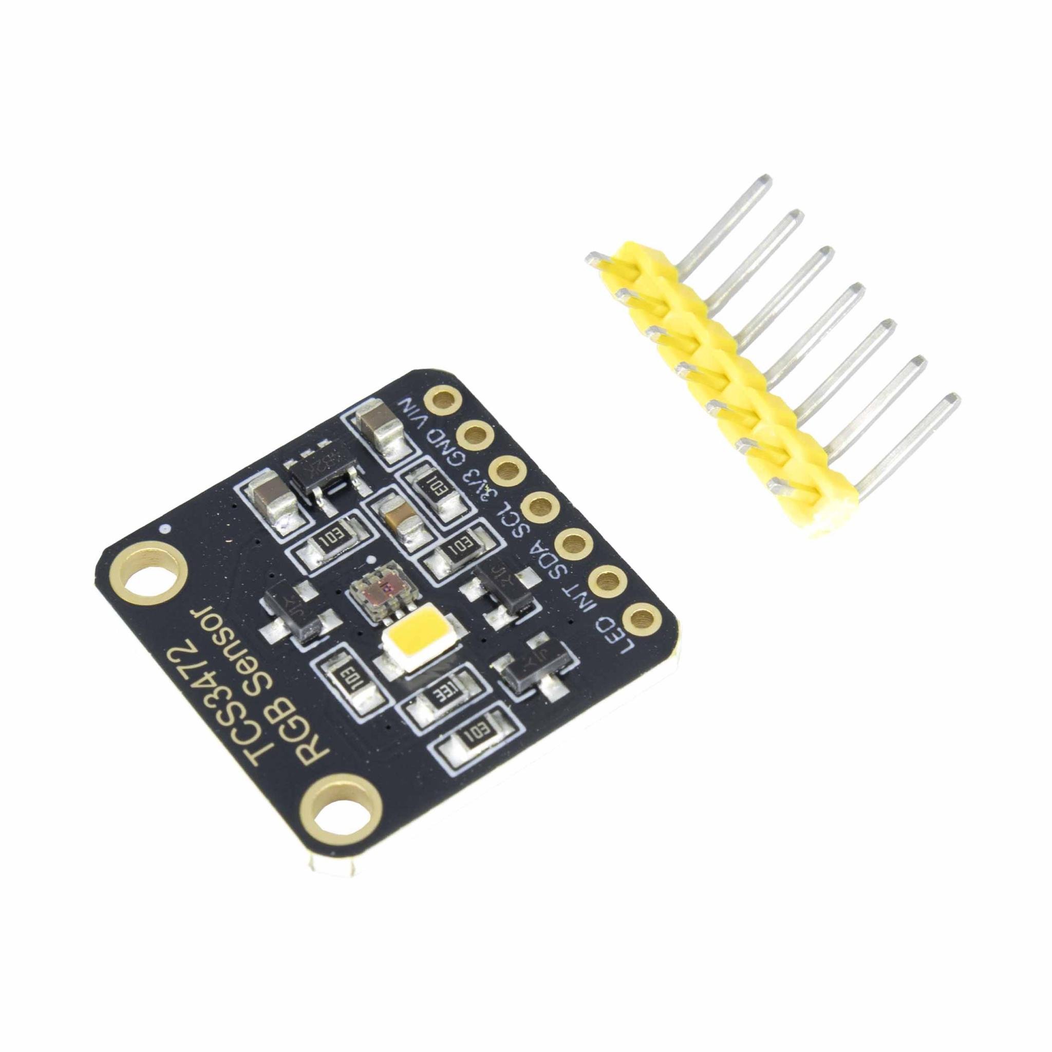

TCS34725 RGB Color Sensor
$2.001 pcs


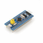


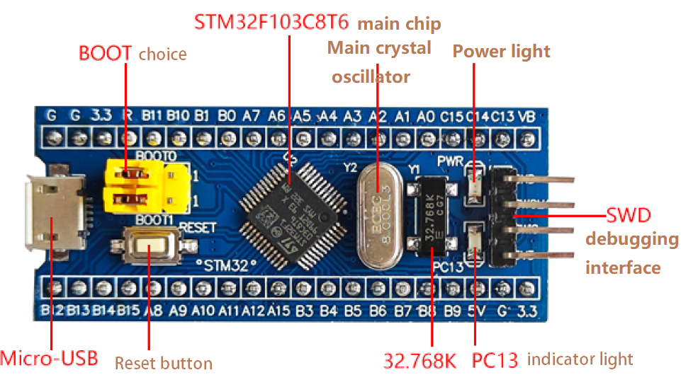
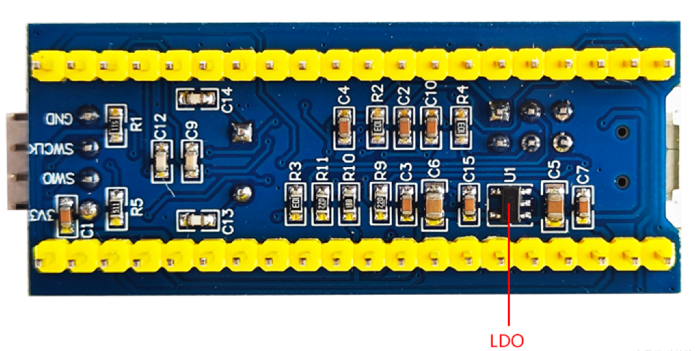
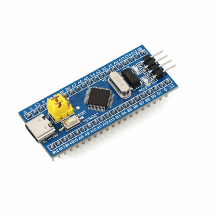
STM32F103C8T6 core board MICRO soldering version
$2.301 pcs
STM32F103C8T6 Micro development board, ARM 32-bit MCU core development board, single-chip microcomputer learning board module.
| Dimensions | 53.34 × 22.86 mm |
|---|---|
| Brand |
easyelecmodule |
1686 in stock


Reviews
There are no reviews yet.