
Blog
Complete Guide to MCP4725 DAC Module 12-bit DAC Development
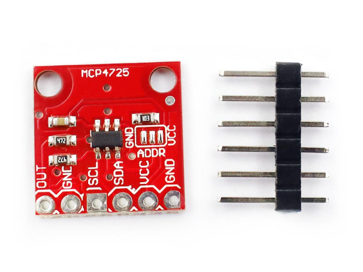
The MCP4725 Digital – to – Analog Converter (DAC) module bridges the gap between the digital world and the analog world, letting your microcontroller (like Arduino or ESP32) produce smooth, adjustable analog voltageswith 12 – bit precision (that’s 4096 steps!). Whether you’re dimming LEDs without flicker, crafting custom audio waves, or simulating sensor outputs, this tiny module packs big controlinto a simple I²C package.
Ready to turn digital commands into perfect analog signals? Let’s dive into how the MCP4725 works, how to wire it, and how to program it for your next project!
What is MCP4725 DAC module?
The MCP4725 is a low-power, high-precision, single-channel 12-bit buffered voltage output Digital-to-Analog Converter (DAC) with Electrically Erasable Programmable Read-Only Memory(EEPROM). Its on-chip precision output amplifier enables it to achieve rail-to-rail analog output swing.
Users can program DAC input and configuration data into the EEPROM using I2C interface commands. The EEPROM function allows the DAC device to retain the DAC input code during power-off, and the DAC output is immediately available after power-up. This function is very useful when the DAC device is used as a supporting device for other devices in the network.
The device includes a Power-On-Reset (POR) circuit to ensure reliable power-up and an on-chip charge pump to provide programming voltage for the EEPROM. The DAC reference voltage is directly driven by VDD. In shutdown mode, the output amplifier can be configured to provide known low, medium, and high resistance output loads. The MCP4725 features an external A0 address bit selection pin. This A0 pin can be connected to VDD or VSS of the user application circuit board.
The MCP4725 has a 2-wire I2C-compatible serial interface, which can be used in standard (100 kHz), fast (400 kHz), or high-speed (3.4 MHz) modes. The MCP4725 is an ideal DAC device for applications with simple design and small form factors, and is suitable for applications that require preserving DAC device settings during power-off.
The MCP4725 DAC module plays a key role in many electronic projects, with typical applications including setting analog outputs of microcontrollers, adjusting LED brightness, and providing precise reference voltages, among others.
MCP4725 Working Principle
MCP4725 Schematic Diagram
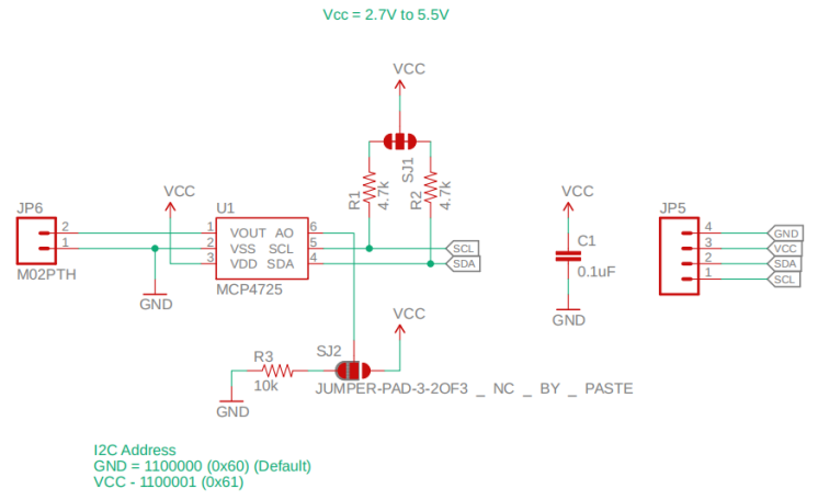
MCP4725 Address
The internal default device address of the chip starts with ‘1100’, A2 and A1 are internally pulled down to ’00’, and A0 is ‘0’ by default, so the default device address is 0x60.

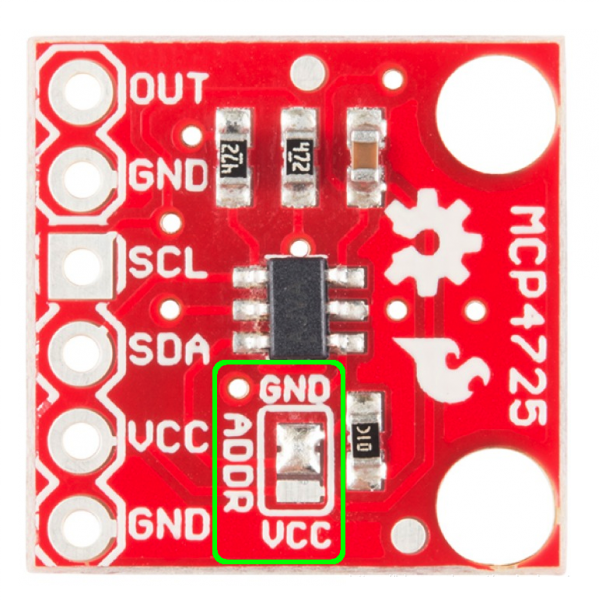
If two MCP4725 modules are used simultaneously, the A0 of one module can be pulled up. The position for modification is shown in the figure below. If the solder is changed to connect ADDR to VCC, the device address will be 0x61.
MCP4725 Output Voltage Encoding Calculation
The MCP4725 is a 12-bit DAC, so its coding range is 0~4096. The relationship between the output voltage value and the code is as follows:

The minimum resolution of the module is related to the supply voltage Vdd. When powered by 5V, the minimum resolution is 1.22mV. The resolution calculation formula is Vdd/4096, as shown in the figure below.

MCP4725 Working Principle
When the device is connected to the I2C bus, it operates as a slave device. Using I2C interface commands, the master device can read/write the DAC input register or EEPROM. The MCP4725 device address includes 4 fixed bits (1100 = device code) and 3 address bits (A2, A1, and A0). The A2 and A1 bits are hardwired before leaving the factory, while the A0 bit is determined by the logic state of the A0 pin. The A0 pin can be connected to VDD or VSS, or effectively driven by a digital logic level. The write command is used to load configuration bits and DAC input codes into the DAC register, or to write to the device’s EEPROM. The write command type is defined by using 3 write command type bits (C2, C1, and C0).

When C2=0 and C1=0, it is the fast mode. This command is used to change the DAC register, and the EEPROM is not affected. When C2=0, C1=1, and C0=0, it is the write DAC register mode, that is, loading configuration bits and data codes into the DAC register. When C2=0, C1=1, and C0=1, it is the write DAC register and EEPROM mode, which loads the configuration bits and data codes into the DAC register and writes them into the EEPROM. This time, the write DAC register mode and the write DAC register and EEPROM mode are mainly used, as shown in the figure below.
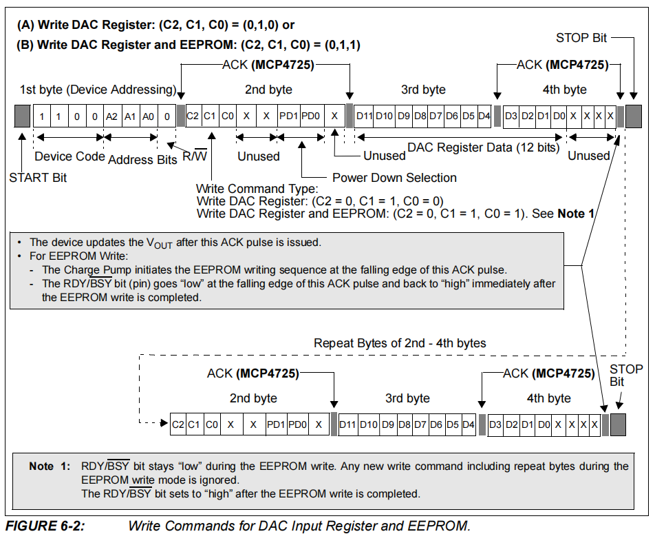
The first byte is the device addressing. A2 and A1 have been set to 0 by the manufacturer, and A0 is controlled by the user (default is 0, grounded), so the first byte is 0x60. The second byte is the write data address. When both PD0 and PD1 are 0, it is the normal mode, so the second byte is 0x60. The 12-bit data input is composed of the third byte and the high 4 bits of the fourth byte, and the input is defined by us.
MCP4725 Parameters
| Parameter | Value |
|---|---|
| Working voltage | +2.7V to +5.5V |
| Resolution | 12bit |
| Operating temperature | -40℃ ~ +125℃ |
| Storage temperature | -65℃ ~ +150℃ |
MCP4725 vs MCP4728
| Model | MCP4725 | MCP4728 |
|---|---|---|
| Number of channels | Single channel (1 analog output) | Four channels (4 independent analog outputs) |
| Application | Simple scenarios (such as a single LED/sensor) | Complex scenarios (such as multi-channel voltage control) |
| I²C address | Fixed or adjustable via the A0 pin (usually 1 address) | Each channel has independent register but shares the I²C address (channels are selected via commands) |
| Price | Cheaper (suitable for low-cost requirements) | Slightly more expensive (more powerful in functionality) |
MCP4725 IC Pin Functions
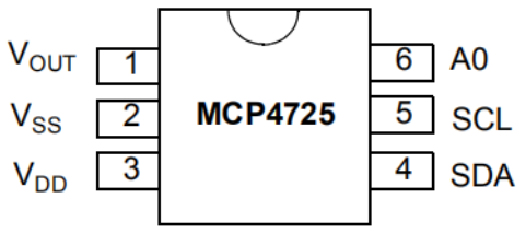
| Pin | Function |
|---|---|
| VOUT | Analog output voltage |
| VSS | Reference ground |
| VDD | Power supply voltage |
| SDA | IIC serial data |
| SCL | IIC serial clock input |
| A0 | IIC address bit selection pin (A0 bit). This pin can be connected to VSS or VDD, or effectively driven by a digital logic level. The logic state of this pin determines the A0 bit of the IIC address bits. |
MCP4725 Feature
- 12-Bit Resolution
- On-Board Non-Volatile Memory (EEPROM)
- ±0.2 LSB DNL (typical)
- External A0 Address Pin
- Normal or Power-Down Mode
- Fast Settling Time: 6 µs (typical)
- External Voltage Reference (VDD)
- Rail-to-Rail Output
- Low Power Consumption
- Single-Supply Operation: 2.7V to 5.5V
- I2C Interface
- Eight Available Addresses
- Standard (100 kbps), Fast (400 kbps), and High-Speed (3.4 Mbps) Modes
- Small 6-lead SOT-23 Package
- Extended Temperature Range: -40°C to +125°C
MCP4725 Arduino Tutorial
MCP4725 Pinout
- MCP4725 Arduino
VCC ——> 3.3V
GND ——> GND
SCL ——> A5
SDA ——> A4
MCP4725 Code
					#include <Wire.h>
#include <Adafruit_MCP4725.h>

Adafruit_MCP4725 dac;

class NormalECG {
private:
  const float targetFreq;  // The frequency of an electrocardiogram (for example, heart rate)
  const int samples;       // Number of sampling points per cycle
  unsigned long startTime; // starting time
  int lastSample;          // The last sampling point
  float scaleFactor;       // The scaling factor of the waveform

public:
  NormalECG(float freq, int smp) : targetFreq(freq), samples(smp) {
    startTime = micros();
    lastSample = 0;
    scaleFactor = 2047.0;  // Used to adjust the amplitude of the waveform
  }

  void update() {
    unsigned long currentTime = micros();
    unsigned long period_us = 1000000 / targetFreq;  // Electrocardiogram cycle (microseconds)
    unsigned long elapsed = currentTime - startTime;

    // Precisely calculate the current sampling point
    int currentSample = (elapsed * samples / period_us) % samples;

    // Update only when necessary
    if (currentSample != lastSample) {
      // Generate simulated electrocardiogram waveforms by combining different sine waves
      float angle = 2.0 * PI * currentSample / samples;

      // P wave: Minor fluctuations
      float ecgValue = 0.4 * sin(angle);

      // QRS complex wave: Rapid peak
      ecgValue += 1.0 * sin(3 * angle);

      // T wave: A relatively gentle fluctuation
      ecgValue += 0.5 * sin(5 * angle);

      // Scale the generated waveform to make it suitable for the output range of the DAC.
      int dacValue = (int)(ecgValue * scaleFactor + 2048);  // Adjust to the center at 2048
      dacValue = constrain(dacValue, 0, 4095); // Ensure that the output value is within the valid range.

      // Output to MCP4725 DAC
      dac.setVoltage(dacValue, false);
      lastSample = currentSample;
    }

    // Prevent overflow of micros()
    if (elapsed > 60000000) {  // Reset in 60 seconds
      startTime = currentTime;
    }
  }
};

// Create a simulation of an electrocardiogram waveform generator, assuming one heartbeat per second.
NormalECG ecgGen(1.0, 500);  // 1 Hz heart rate, 500 sampling points

void setup() {
  Serial.begin(9600);
  Wire.begin();

  if (!dac.begin(0x60)) {
    if (!dac.begin(0x62)) {
      Serial.println("MCP4725 not found!");
      while(1);
    }
  }

  Serial.println("The simulated electrocardiogram generator is ready.");
}

void loop() {
  ecgGen.update();  // Continuously update the simulated electrocardiogram waveform.
}
MCP4725 Effect Demonstration
MCP4725 Application Scenario
- Set Point or Offset Trimming
- Sensor Calibration
- Closed-Loop Servo Control
- Low Power Portable Instrumentation
- PC Peripherals
- Data Acquisition Systems
Relative Information
Purchase Link
FAQ
What is the output range of the MCP4725?
The output voltage is a rail-to-rail output and is proportional to the power supply pin. Therefore, if a 3.3V power supply is used, the output range is 0-3.3V. If a 5V power supply is used, the output range is 0-5V.
What should we do if the output voltage of MCP4725 is unstable/noisy?
① Power supply interference
Solution: Ensure stable VCC power supply (it is recommended to use a linear regulated power supply instead of a switching power supply directly). Connect a 0.1μF ceramic capacitor and a 10μF electrolytic capacitor in parallel between VCC and GND (to filter out high-frequency and low-frequency noise).
② I²C communication issues
Solution: Check if the SDA/SCL lines are too long (it is recommended to be ≤ 30cm). If necessary, add pull-up resistors (usually 4.7kΩ-10kΩ, connecting SDA/SCL to VCC).
③ Code logic problems
Solution: Ensure that the parameters of the setVoltage() function are correct (e.g., digitalValue does not exceed 4095), and avoid frequent writing to prevent module overload.
④ Module quality issues
Solution: Try replacing the MCP4725 module or check if the solder joints are cold-soldered.
