Blog
STM32F103C8T6 Development Board: A Comprehensive Guide for Embedded Enthusiasts

Introduction
In the field of embedded development, STM32 series microcontrollers have become the top choice for engineers and hobbyists due to their powerful performance, rich peripherals, and excellent cost-effectiveness. Among them, the STM32F103C8T6 development board stands out as a popular option for getting started with STM32, thanks to its affordable price, compact design, and outstanding compatibility. This article will comprehensively break down this classic development board—from chip comparisons and hardware analysis to parameter specifications, circuit principles, and practical projects—to help you quickly get started with development.
Core Parameter Comparison of STM32 Series Chips
The STM32F1 series includes multiple sub-models, with differences in Flash capacity, pin count, and peripheral configurations. Below is a comparison of popular models related to the STM32F103C8T6, helping you choose based on project requirements:


| CHIP MODEL | FLASH CAPACITY | SRAM CAPACITY | PIN COUNT | PERIPHERAL HIGHLIGHTS | APPLICATION SCENARIOS | REFERENCE PRICE RANGE |
|---|---|---|---|---|---|---|
| STM32F103C8T6 | 64KB | 20KB | 48 | USB, CAN, 2 ADCs, 3 USARTs | Entry-level Development, Small Control Projects | $0.09-$0.91 |
| STM32F103C6T6 | 32KB | 10KB | 48 | Basic Peripherals, No USB/CAN | Minimalist Control Scenarios, Cost-Sensitive Projects | $0.08-$0.50 |
| STM32F103CBT6 | 128KB | 20KB | 48 | Enhanced Peripherals, Larger Flash | Complex Algorithms, Multi-Peripheral Interaction Projects | $0.15-$1.20 |
| STM32F103RCT6 | 256KB | 48KB | 64 | More GPIOs, 3 SPIs | Medium to Large Control Projects, Multi-Sensor Interaction | $0.12-$1.50 |
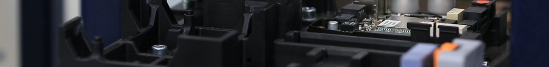
Introduction to Core Components of the STM32F103C8T6 Development Board
The main components of the board are shown in the figure below, including the microcontroller (MCU), power supply, buttons, crystal oscillators, and programming interface pins:
1.Main Control Chip: STM32F103C8T6
As the “brain” of the development board, the STM32F103C8T6 is based on the Arm® Cortex®-M3 core, with a maximum frequency of 72 MHz and a computing performance of 1.25 DMIPS/MHz. It supports single-cycle multiplication and hardware division, and includes 64KB of Flash (for program storage) and 20KB of SRAM (for data caching)—sufficient for most entry-level embedded projects. The chip supports a wide supply voltage range of 2.0–3.6 V and three low-power modes (Sleep, Stop, Standby), making it suitable for battery-powered devices.
2.Key Peripheral Components
- Micro-USB/Type-C Interface:Primarily used for power supply (can also support UART communication expansion in some cases). It connects the development board to a computer or 5V power adapter via a USB cable to provide 5V input voltage. The onboard voltage regulator circuit converts the voltage to power the chip and peripherals..
- LDO (Low-Dropout Regulator): The on-board AMS1117-3.3V LDO chip converts the 5V input voltage to a stable 3.3V output. It powers the STM32F103C8T6 main chip and other 3.3V-compatible peripherals (likesome sensors, debugging interfaces). Compared to ordinary linear regulators, the LDO features low dropout voltage, low power consumption, and low output ripple—effectively ensuring power stability and avoiding interference from voltage fluctuations on system operation and peripheral communication.
- Reset Circuit: Consists of a 10KΩpull-up resistor and a 0.1μFfilter capacitor, forming a simple and reliable reset circuit to ensure stable startup of the chip when powered on.
- Clock Circuit:Equipped with an 8MHzexternal crystal oscillator (HSE) and a 32.768KHz real-time clock (RTC) crystal oscillator (LSE). These work with the chip’s internal RC oscillator to provide accurate clock signals for the system.
- Programming Interface: SupportsSWD (Serial Wire Debug) mode, which requires only 2 wires to implement program downloading and on-line debugging—simplifying the development process.
- BOOT Selection:The chip’s startup mode is selected by configuring the voltage levels of the BOOT0 and BOOT1pins. For example:By default, BOOT0 is connected to GND (0V) and BOOT1 to GND (0V), so the chip starts from the user Flash (normal operation mode).To enter Bootloader mode (for program updates), connect BOOT0 to VCC (3.3V) and BOOT1 to GND. After power-on, programs can be downloaded via USART1.
STM32FC103C8T6 Datasheet
The following is a summary of the most commonly used key information in development. If you want to learn more details, you can refer to this website.
| PARAMETER CATEGORY | SPECIFIC SPECIFICATIONS |
|---|---|
| Core Parameters | Cortex-M3 Core, Maximum Frequency 72MHz, 1.25 DMIPS/MHz |
| Storage Capacity | 64KB Flash (Program Storage), 20KB SRAM (Data Cache) |
| Power Supply Voltage | Board-level Input 5V (USB/DC), Chip Core 3.3V (2.0-3.6V Wide Voltage Compatible) |
| Operating Temperature | -40°C ~ +105°C (Industrial Temperature Range) |
| Peripheral Configuration | 2 × 12-bit ADC (up to 16 channels), 3 × USART, 2 × I2C, 2 × SPI, 1 × USB 2.0 Full-Speed, 1 × CAN 2.0B |
| GPIO Resources | 37 General-Purpose I/O Ports, Almost All Support 5V, Configurable as Input / Output / Alternate Function |
STM32F103C8T6 Pinout and Schematic Diagram


The STM32F103C8T6 development board has rich pin functions, including power pins, digital I/O pins, analog input pins, and communication peripheral pins. Below is a detailed breakdown by port group:
Power Pins
- +5V: External 5V power input (via Micro-USB or external power supply).
- +3.3V:3.3V regulated output from the on-board LDO (AMS1117), powering the chip and 3.3V-compatible peripherals.
- GND: Power ground, the common reference ground for all circuits.
- +3.3V (external in): External 3.3V power input interface (for external power supply if needed).
GPIO Ports (Digital I/O and Alternate Functions)
The STM32F103C8T6 has three general-purpose I/O ports: GPIOA, GPIOB, and GPIOC. Each pin can be configured as digital input/output or reused for communication, analog, or other functions.
- GPIOA Port (PA0~PA15)
| PIN | DIGITAL I/O FUNCTION | ALTERNATE FUNCTION (TYPICAL SCENARIO) |
|---|---|---|
| PA0 | Digital Input / Output | ADC1 Channel 0 (Analog Input), TIM2_CH1 (Timer Input Capture) |
| PA1 | Digital Input / Output | ADC1 Channel 1 (Analog Input), TIM2_CH2 (Timer Input Capture) |
| PA2 | Digital Input / Output | USART2_TX (UART2 Transmit), SPI2_MOSI (SPI2 Master Output Slave Input) |
| PA3 | Digital Input / Output | USART2_RX (UART2 Receive), SPI2_MISO (SPI2 Master Input Slave Output) |
| PA4 | Digital Input / Output | SPI1_NSS (SPI1 Slave Select), ADC1 Channel 4 (Analog Input) |
| PA5 | Digital Input / Output | SPI1_SCK (SPI1 Clock), ADC1 Channel 5 (Analog Input) |
| PA6 | Digital Input / Output | SPI1_MISO (SPI1 Master Input Slave Output), ADC1 Channel 6 (Analog Input) |
| PA7 | Digital Input / Output | SPI1_MOSI (SPI1 Master Output Slave Input), ADC1 Channel 7 (Analog Input) |
| PA8 | Digital Input / Output | TIM1_CH1 (Timer 1 Channel 1), MCO (Main Clock Output) |
| PA9 | Digital Input / Output | USART1_TX (UART1 Transmit), USB_VBUS (USB Bus Detection) |
| PA10 | Digital Input / Output | USART1_RX (UART1 Receive) |
| PA11 | Digital Input / Output | USB_DM (USB Differential Negative), CAN1_RX (CAN Bus Receive) |
| PA12 | Digital Input / Output | USB_DP (USB Differential Positive), CAN1_TX (CAN Bus Transmit) |
| PA13 | Digital Input / Output | SWDIO (SWD Debug Data) |
| PA14 | Digital Input / Output | SWCLK (SWD Debug Clock) |
| PA15 | Digital Input / Output | SPI1_NSS (SPI1 Slave Select), TIM2_CH1 (Timer 2 Channel 1) |
- GPIOB Port (PB0~PB15)
| PIN | DIGITAL I/O FUNCTION | ALTERNATE FUNCTION (TYPICAL SCENARIO) |
|---|---|---|
| PB0 | Digital Input / Output | ADC1 Channel 8 (Analog Input), TIM3_CH3 (Timer 3 Channel 3) |
| PB1 | Digital Input / Output | ADC1 Channel 9 (Analog Input), TIM3_CH4 (Timer 3 Channel 4) |
| PB2 | Digital Input / Output | BOOT1 (Boot Mode Selection) |
| PB3 | Digital Input / Output | JTDO (JTAG Debug), TIM2_CH2 (Timer 2 Channel 2) |
| PB4 | Digital Input / Output | JTRST (JTAG Reset), TIM3_CH1 (Timer 3 Channel 1) |
| PB5 | Digital Input / Output | I2C1_SMBUS (SMBus Protocol), TIM3_CH2 (Timer 3 Channel 2) |
| PB6 | Digital Input / Output | I2C1_SCL (I2C1 Clock), TIM4_CH1 (Timer 4 Channel 1) |
| PB7 | Digital Input / Output | I2C1_SDA (I2C1 Data), TIM4_CH2 (Timer 4 Channel 2) |
| PB8 | Digital Input / Output | TIM4_CH3 (Timer 4 Channel 3), I2C2_SCL (I2C2 Clock) |
| PB9 | Digital Input / Output | TIM4_CH4 (Timer 4 Channel 4), I2C2_SDA (I2C2 Data) |
| PB10 | Digital Input / Output | USART3_TX (UART3 Transmit), I2C2_SCL (I2C2 Clock) |
| PB11 | Digital Input / Output | USART3_RX (UART3 Receive), I2C2_SDA (I2C2 Data) |
| PB12 | Digital Input / Output | SPI2_NSS (SPI2 Slave Select), TIM1_CH1 (Timer 1 Channel 1) |
| PB13 | Digital Input / Output | SPI2_SCK (SPI2 Clock), TIM1_CH1N (Timer 1 Complementary Channel 1) |
| PB14 | Digital Input / Output | SPI2_MISO (SPI2 Master Input Slave Output), TIM1_CH2N (Timer 1 Complementary Channel 2) |
| PB15 | Digital Input / Output | SPI2_MOSI (SPI2 Master Output Slave Input), TIM1_CH3N (Timer 1 Complementary Channel 3) |
- GPIOC Port (PC13~PC15)
| PIN | DIGITAL I/O FUNCTION | ALTERNATE FUNCTION (TYPICAL SCENARIO) |
|---|---|---|
| PC13 | Digital Input / Output | On-board LED Indicator (Default Function), RTC_TAMPER (RTC Tamper Prevention) |
| PC14 | Digital Input / Output | LSE (32.768KHz Crystal Input) |
| PC15 | Digital Input / Output | LSE (32.768KHz Crystal Output) |
Analog Input Pins (ADC)
The STM32F103C8T6 includes 2×12-bit ADCs, supporting up to 16 analog input channels. Common analog input pins are:
PA0~PA7, PB0~PB1: Can be used as analog input channels for ADC1 (like connecting potentiometers, temperature sensors, or other analog devices).
Communication Peripheral Pins
UART (USART)
- USART1: PA9 (TX), PA10 (RX)→ High-speed UART, suitable for debugging prints and long-distance communication.
- USART2:PA2 (TX), PA3 (RX)→ Medium-speed UART, connectable to Bluetooth, GPS, or other modules.
- USART3: PB10 (TX), PB11 (RX)→ Medium-speed UART, ideal for multi-peripheral expansion.
I2C Bus
- I2C1: PB6 (SCL), PB7 (SDA)→ Connectable to I2C devices such as OLED displays, temperature-humidity sensors (likeDHT11, BH1750).
- I2C2: PB10 (SCL), PB11 (SDA)→ Additional I2C bus for multi-device parallel connections.
SPI Bus
- SPI1: PA4 (NSS), PA5 (SCK), PA6 (MISO), PA7 (MOSI) → High-speed SPI, connectable to SPI displays, SD card modules, etc.
- SPI2:PB12 (NSS), PB13 (SCK), PB14 (MISO), PB15 (MOSI) → Medium-speed SPI for peripheral expansion.
USB Bus
- USB_DM (PA11), USB_DP (PA12):USB 2.0 Full-Speed interface, supporting virtual UART, HID devices (likecustom keyboards/mice), etc.
CAN Bus
- CAN1_TX (PA12), CAN1_RX (PA11):CAN 2.0B bus interface, suitable for multi-node communication in industrial control or automotive electronics.
Timer and PWM Pins
The STM32F103C8T6 includes multiple timers that output PWM waveforms, commonly used for motor driving, LED dimming:
- TIM2: PA0 (CH1), PA1 (CH2), PA2 (CH3), PA3 (CH4)
- TIM3: PB0 (CH3), PB1 (CH4), PB4 (CH1), PB5 (CH2)
- TIM4:PB6 (CH1), PB7 (CH2), PB8 (CH3), PB9 (CH4)
- TIM1:PA8 (CH1), PA9 (CH2), PA10 (CH3), PB13 (CH1N), PB14 (CH2N), PB15 (CH3N)
By understanding these pin functions, you can flexibly configure hardware connections for your project needs—whether it’s basic tasks like LED displays or sensor data collection, or advanced applications such as serial communication or USB development. The STM32F103C8T6 development board provides plentiful support for all these requirements.
Detailed Explanation of Key Circuits on the STM32F103C8T6 Development Board
The minimum system of a microcontroller refers to the minimal circuit required to ensure the MCU operates normally. The STM32 minimum system typically includes a power circuit, crystal oscillator (clock) circuit, reset circuit, programming/debugging circuit, BOOT startup circuit, and filter circuit. Its schematic diagram is shown below:
Power Circuit
The board uses two voltage levels: 5V (VCC_5V) and 3.3V (VCC_3V3):
- 5V: Powers external modules that require 5V (like stepper motors, DC motors).
- 3.3V:Powers the microcontroller, LEDs, and 3.3V-compatible external modules (liketemperature sensors).
Crystal Oscillator (Clock) Circuit
- High-Speed External Clock (HSE):An8MHz crystal oscillator, paired with two 22pF load capacitors, connects to the MCU’s OSC_IN (PD0) and OSC_OUT (PD1) pins. It provides a high-precision、high-speed clock for the system and supports PLL frequency multiplication up to 72MHz.
- Low-Speed External Clock (LSE):A 32.768KHzcrystal oscillator, paired with two 15pF load capacitors, connects to PC14 (OSC32_IN) and PC15 (OSC32_OUT) pins. It is used for the RTC to implement timekeeping functions.
Reset Circuit
- Uses a “pull-up resistor + capacitor” design: A10KΩpull-up resistor pulls the NRST pin to 3.3V, and a 0.1μF capacitor is connected to ground.
- When powered on, the capacitor charges, keeping theNRSTpin low for a short period to allow the chip to complete reset initialization. Pressing the reset button manually pulls the NRST pin low to trigger a manual reset.
Programming/Debugging Circuit
- Adopts the SWD (Serial Wire Debug) interface, which requires only two wires (SWCLKfor clock and SWDIOfor data), plus GND and 3.3V power, to connect to an ST-Link V2 debugger.
- Compared to the traditionalJTAGinterface, the SWD interface uses fewer pins and offers faster download speeds. It is the mainstream debugging method for STM32F103C8T6 Blue Pill boards, supporting program downloading, breakpoint debugging, and register inspection.

STLINK Debugging Tool and STM32F103C8T6 Wiring Configuration:
| STM32F103C8T6 MINIMUM SYSTEM BOARD | SIMPLE STM32 DOWNLOADER |
|---|---|
| 3V3 | 3.3V |
| SWIO | SWDIO |
| SWCLK | SWCLK |
| GND | GND |
BOOT Startup Circuit
- The development board selects the boot mode through the voltage levels of pins BOOT0 and BOOT1. By default, BOOT0is connected to GND (0V)and BOOT1 to GND (0V), enabling boot from the user’s Flash memory (normal operating mode).
- To enter bootloader mode (procedure upgrade), connectBOOT0 to VCC(3.3V and BOOT1 to GND. After power-on, download theprocedure via USART1.
Introduction to three startup modes of microcontroller:
| BOOT MODE SELECTION PIN LEVELS | BOOT MODE | 0X00000000 MAPPING ADDRESS | 0X00000004 MAPPING ADDRESS | |
|---|---|---|---|---|
| BOOT0 | BOOT1 | |||
| 0 | x | Internal FLASH | 0x08000000 | 0x08000004 |
| 1 | 1 | Internal SRAM | 0x20000000 | 0x20000004 |
| 1 | 0 | System Memory | 0x1FFF0000 | 0x1FFF0004 |
6.Filter Circuit
- Power Decoupling:0.1μFceramic capacitors are connected in parallel near the chip’s power pins (VDD, VDDA) for decoupling and filtering, reducing noise on the power line that could interfere with the chip’s core circuits.
- ADC Reference Voltage Filter: 10nF + 1μFfilter capacitors are connected to the ADC reference voltage pin (VREF+) to ensureADC conversion accuracy, especially in analog signal acquisition scenarios.
Detailed Comparison: STM32F103C8T6 vs. STM32F103C6T6 vs. STM32F103CBT6
All three chips belong to the STM32F103 series and are pin-compatible, but differ significantly in core configurations:
| COMPARISON DIMENSION | STM32F103C8T6 (BLUE PILL CORE) | STM32F103C6T6 | STM32F103CBT6 |
|---|---|---|---|
| Storage Capacity | 64KB Flash + 20KB SRAM | 32KB Flash + 10KB SRAM | 128KB Flash + 20KB SRAM |
| Core Peripherals | 1×USB 2.0 Full-Speed, 1×CAN 2.0B, 3×USART, 2×I2C, 2×SPI | 3×USART, 1×I2C, 1×SPI, No USB/CAN | 1×USB 2.0 Full-Speed, 1×CAN 2.0B, 3×USART, 2×I2C, 2×SPI |
| ADC Configuration | 2×12-bit ADC, up to 16 channels | 2×12-bit ADC, up to 10 channels | 2×12-bit ADC, up to 16 channels |
| Computing Performance | 72MHz Frequency, 1.25 DMIPS/MHz | 72MHz Frequency, 1.25 DMIPS/MHz | 72MHz Frequency, 1.25 DMIPS/MHz |
| Supply Voltage | 2.0-3.6V | 2.0-3.6V | 2.0-3.6V |
| Operating Temperature | -40°C~+105°C | -40°C~+105°C | -40°C~+105°C |
| Price Advantage | Highest cost-performance, balances performance and cost | Lowest price, first choice for cost-sensitive scenarios | Slightly higher price, first choice for large program storage needs |
| Compatibility | Can directly replace C6T6, note Flash capacity | Pin-compatible, function reduced | Can directly replace C8T6, Flash capacity doubled |
Practical Project: Running a Flowing LED Project with the STM32F103C8T6
The flowing LED project is the “Hello World” of embedded development. Below is a complete implementation process based on STM32CubeIDE, suitable for beginners:
Preparation Tools
- Hardware: STM32F103C8T6 (Blue Pill) development board, ST-Link V2 debugger, USB cable, 4 LEDs, 4×220Ω current-limiting resistors, breadboard, and jumper wires.
- Software: STM32CubeIDE (integrates compilation and downloading functions), STM32F103C8T6 datasheet.
Hardware Wiring
- Connect the anodes of the 4 LEDs to pins PB0, PB1, PB2, and PB3 via 220Ω resistors.
- Connect the cathodes of the LEDs to the development board’s GND pin.
- Connect the ST-Link V2 debugger to the development board via SWD wires: SWCLK → PA14, SWDIO → PA13, GND → GND, 3.3V → 3.3V.
- Connect the development board’s 5V interface to a computer via a USB cable to supply power.
Software Development Steps
Step 1: Create a Project
- Open STM32CubeIDE, create a new project, search for the “STM32F103C8T6” chip, and select the corresponding model.
- Configure the clock: Set HSE to 8MHz, enable PLL to multiply the frequency to72MHz, set APB1 clock to 36MHz, and APB2 clock to 72MHz.
- Configure GPIOs: Set PB0–PB3 to output mode (push-pull output, no pull-up/down resistors).
Step 2: Write Code
Add the flowing LED logic to the while(1) loop in the main.c file:
					while (1)
{
  // Turn on LEDs one by one
  HAL_GPIO_WritePin(GPIOB, GPIO_PIN_0, GPIO_PIN_SET);
  HAL_Delay(500); // Delay 500ms
  HAL_GPIO_WritePin(GPIOB, GPIO_PIN_1, GPIO_PIN_SET);
  HAL_Delay(500);
  HAL_GPIO_WritePin(GPIOB, GPIO_PIN_2, GPIO_PIN_SET);
  HAL_Delay(500);
  HAL_GPIO_WritePin(GPIOB, GPIO_PIN_3, GPIO_PIN_SET);
  HAL_Delay(500);

  // Turn off LEDs one by one
  HAL_GPIO_WritePin(GPIOB, GPIO_PIN_0, GPIO_PIN_RESET);
  HAL_Delay(500);
  HAL_GPIO_WritePin(GPIOB, GPIO_PIN_1, GPIO_PIN_RESET);
  HAL_Delay(500);
  HAL_GPIO_WritePin(GPIOB, GPIO_PIN_2, GPIO_PIN_RESET);
  HAL_Delay(500);
  HAL_GPIO_WritePin(GPIOB, GPIO_PIN_3, GPIO_PIN_RESET);
  HAL_Delay(500);
}
Step 3: Program Download and Debugging
- Connect the ST-Link V2 to the computer. In STM32CubeIDE, configure the debugger as “ST-Link Debugger”.
- Click the “Run” button:The program will automatically compile and download to the development board. The LEDs will then light up and turn off in sequence, achieving the flowing effect.
Project Expansion
- Adjust the flowing speed by modifying the HAL_Delay()parameter.
- Integrate ADCfunctionality to control the flowing speed using a potentiometer.
- Use USART1to control LED on/off via serial commands from a computer’s serial assistant.
FAQS
Why Can’t I Download Programs to the STM32F103C8T6 Blue Pill Development Board?
- Check if the SWD wiring is correct(SWCLK → PA14, SWDIO → PA13)and ensure stable GND and 3.3V power supply.
- Verify the BOOT mode configuration: EnsureBOOT0 = GND、BOOT1 = GND(normal startup from Flash). Incorrect settings will prevent startup from Flash.
- Check if the ST-Link V2 driveris installed correctly: Verify recognition in the computer’s Device Manager.
Why Doesn’t the LED Light Up After Powering On the Development Board?
- Power Supply Issues: Check if the USB cable is intact, if 5V power is normal, and if the AMS1117-3.3Vchip is overheating (overheating may indicate a short circuit).
- Code Logic Issues:Confirm correctGPIO pin configuration and check if the HAL_GPIO_WritePin function uses the correct pin numbers and voltage levels.
- Hardware Wiring Errors:Ensure the LED’s anode/cathode are not reversed, and that current-limiting resistors are properly soldered.
How to Use the USB Function of the STM32F103C8T6?
- Configure the USB peripheral as “USB Device” in STM32CubeMX and select the corresponding USB class (like virtual UART, HID device).
- Ensure hardware connections: Check that PA11 (USB_DM)and PA12 (USB_DP)pins are properly soldered and that the USB cable is connected correctly.
- Download the USB firmware library and configure USB-related code according to examples to implement USB communication.
Does the STM32F103C8T6 Blue Pill Development Board Support Arduino Development?
Yes! Add the STM32 development board to Arduino IDE (search for “STM32F1” in Board Manager).Select the “Generic STM32F103C8” board and configure the upload method as “ST-Link”. You can then write code using Arduino syntax and download it.
How to Reduce Power Consumption of the STM32F103C8T6 Development Board?
- Use Stop Mode: Disable unnecessary peripheral clocks and retain only RTC or external interrupt wake-up sources.
- Lower the system clock: Reduce the frequency from 72MHzto a lower value (like8MHz) to reduce CPU computing power consumption.
- Optimize GPIO configuration:Set unused GPIO to input mode with pull-down resistors to avoid power consumption from floating pins.