blog

What Need to Consider When Designing a BMS, and How to Design It?

1111111111111111

Is Choosing the Right Chips Half the Battle Won?

Well, sort of, but not entirely. The AFE (Analog Front-End), MCU (Microcontroller Unit), and fuel gauge in a BMS may seem like three independent chips, but in practice, you need them to work together like a “team”—the connection between each link is crucial.
 
Many people, when starting to choose chips, fixate on the sampling accuracy of the AFE and the computing power of the MCU. Yet, they only find out after soldering the board that the data collected by the AFE can’t be transmitted to the fuel gauge, or the AFE doesn’t respond to the commands sent by the MCU. This happens because they didn’t clarify the division of labor between the three. Actually, it’s quite simple:
 
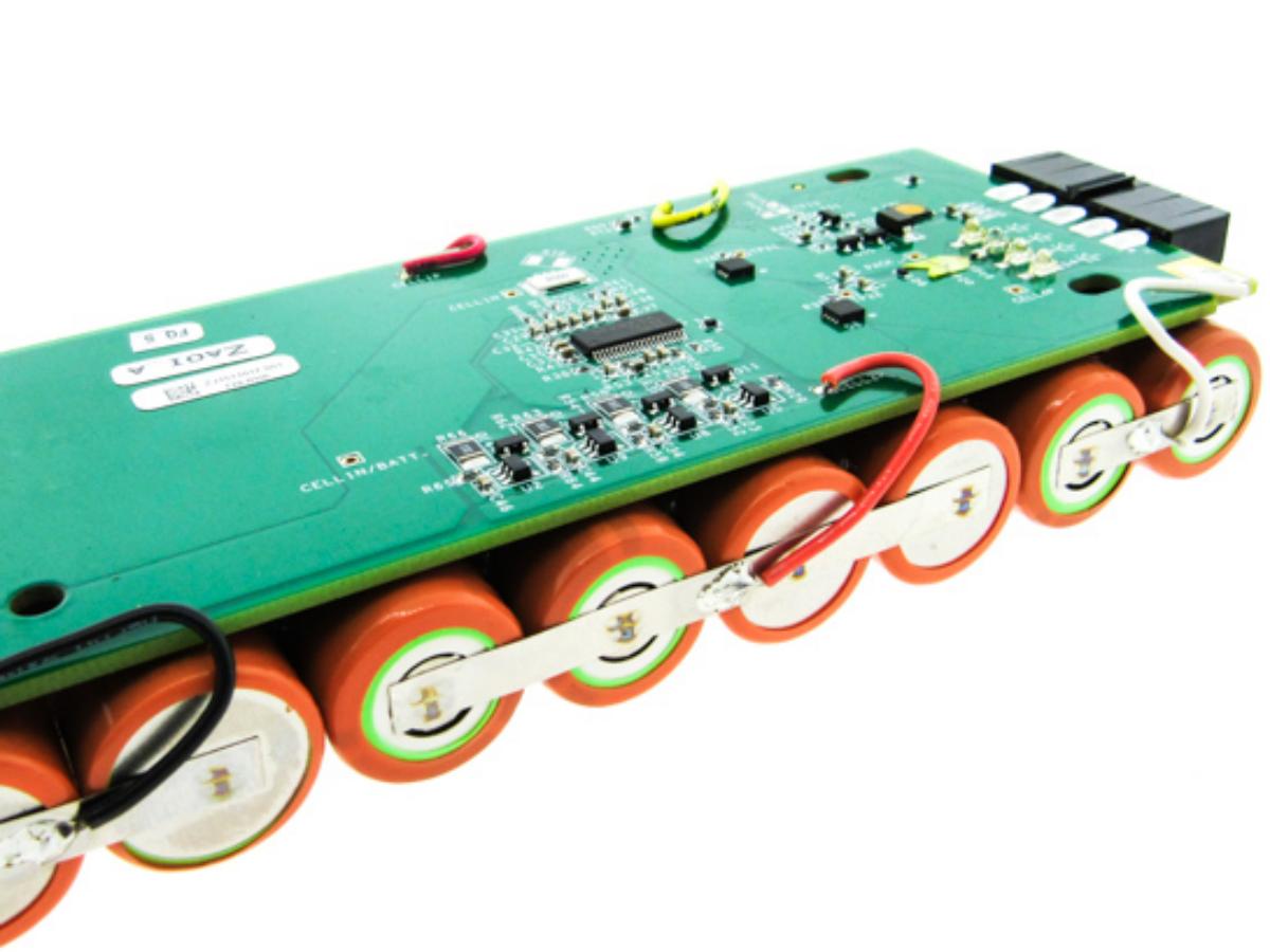
  • The AFE is “the one on the front lines”—it’s closest to the battery and responsible for accurately collecting data like voltage, current, and temperature. It also needs to make quick decisions in emergencies; for example, if the battery shorts, it can’t wait for the MCU’s approval but must cut off the circuit directly. A split second of delay could cause the battery to bulge.
  • The MCU is “the coordinator”—it integrates the raw data from the AFE and the SOC (State of Charge) calculated by the fuel gauge, then tells the charger “it’s time to reduce power” or sends a signal to the instrument panel saying “how much power is left.”
  • The fuel gauge is “the translator”—it converts the “how many volts, how many amps” collected by the AFE into understandable info like “30% power remaining” or “the battery will last another 2 years.” If its calculations are inaccurate, users will feel like “the range is falsely advertised.”
So when choosing chips, don’t just look at individual parameters. First, you need to figure out how these three chips will work together.
图片1 29

Replace the AFE When SOC Accuracy Is Insufficient?

If you can’t get the SOC accuracy up, the problem might not be with the AFE. Many people think that as long as the AFE has high accuracy, the SOC will definitely be accurate—but that’s not the case.
 
Take a phone battery as an example: the relationship between voltage and capacity changes at low temperatures. For instance, at room temperature, 3.8V corresponds to 50% SOC, but at -10°C, 3.8V might only mean 40% remaining. If the fuel gauge still uses the room-temperature model, the calculated SOC will definitely be inaccurate. So during design, you need to make the fuel gauge adapt to the battery’s “temperament.” First, test the battery’s characteristic data under different temperatures and discharge currents, then calibrate the model based on this data—don’t just use the general model that comes with the chip. This way, you can improve the SOC accuracy.
 
Relying solely on a coulomb counter will lead to the accumulation of current measurement errors, which in turn causes SOC drift. There are usually two types of compensation for this:
 
  1. OCV (Open Circuit Voltage) calibration: When the battery is idle for ≥2 hours (OCV stabilizes), use the OCV value to correct the SOC. If the calibration deviation exceeds 3%, trigger a parameter reset.
  2. ESR (Equivalent Series Resistance) compensation: Based on the voltage and current data collected synchronously by the AFE, calculate ESR changes in real time to correct the impact of voltage drop under dynamic loads on SOC estimation.
There’s another detail easily overlooked: the sampling synchronization of the AFE. If voltage and current aren’t sampled at the same time, the calculated battery internal resistance (ESR) will have a large deviation, which then affects the SOC. Here are two issues you need to consider:
 
First is the hardware-level synchronization design. You need to ensure that the timestamps of voltage and current sampling are consistent to avoid ESR calculation errors caused by timing deviations. For example, use the same clock signal to trigger the voltage ADC (Analog-to-Digital Converter) and current ADC, so that the sampling time difference is ≤100μs—at this point, the ESR estimation error can be controlled within 5%. If sampling is asynchronous (e.g., a time difference of 1ms), the ESR error will exceed 20%, which in turn increases the dynamic SOC error by 3%-4%.
 
Second is the scenario adaptation of sampling frequency. Too high a sampling frequency increases power consumption, while too low a frequency misses transient fluctuations. You can adjust it according to load characteristics:
 
  • For consumer electronics, use 10Hz to balance accuracy and power consumption.
  • For energy storage systems (e.g., home energy storage), use 50Hz to capture current mutations during charge-discharge switching.
  • For automotive scenarios, use 100Hz to adapt to rapid current changes during regenerative braking.
So when adjusting SOC accuracy, don’t just rush to replace it with a high-precision AFE. Be sure to check if the fuel gauge’s model is correct and if the AFE sampling is synchronized.
图片2 24

If a Fault Occurs, Should You Cut Off Power Directly?

What would you do if a BMS fault occurs? Do you think that no matter what, cutting off power immediately will solve the problem once and for all and ensure safety? This simple and rough method is indeed convenient and reassuring—especially when the BMS has a short circuit and the current suddenly surges. The battery risks overheating, bulging, or exploding in an instant, so cutting off power directly is necessary. But sometimes, the fault isn’t that serious, and there’s no need for an all-or-nothing power cut. It not only disrupts usage but also has no real effect. It’s more practical to classify faults (into emergency, severe, minor, etc.) when handling them. For example, at what temperature a small fan should be used for cooling, and at what temperature power must be cut off immediately—these all need to be decided based on actual conditions. When the battery voltage drops below a certain level, the MCU should first remind the user “it’s time to charge” instead of shutting down directly. This way, you ensure safety without compromising the user experience.
 
The choice between high-side and low-side protection also depends on the scenario:
 
  • For high-power projects like automotive or energy storage, prioritize high-side protection. Although you need to install an additional charge pump to drive the MOSFET, the grounding is stable—and even if a fault occurs, communication won’t be interrupted.
  • For low-power devices like phones or earbuds, low-side protection is more convenient. No extra components are needed, and it saves costs.

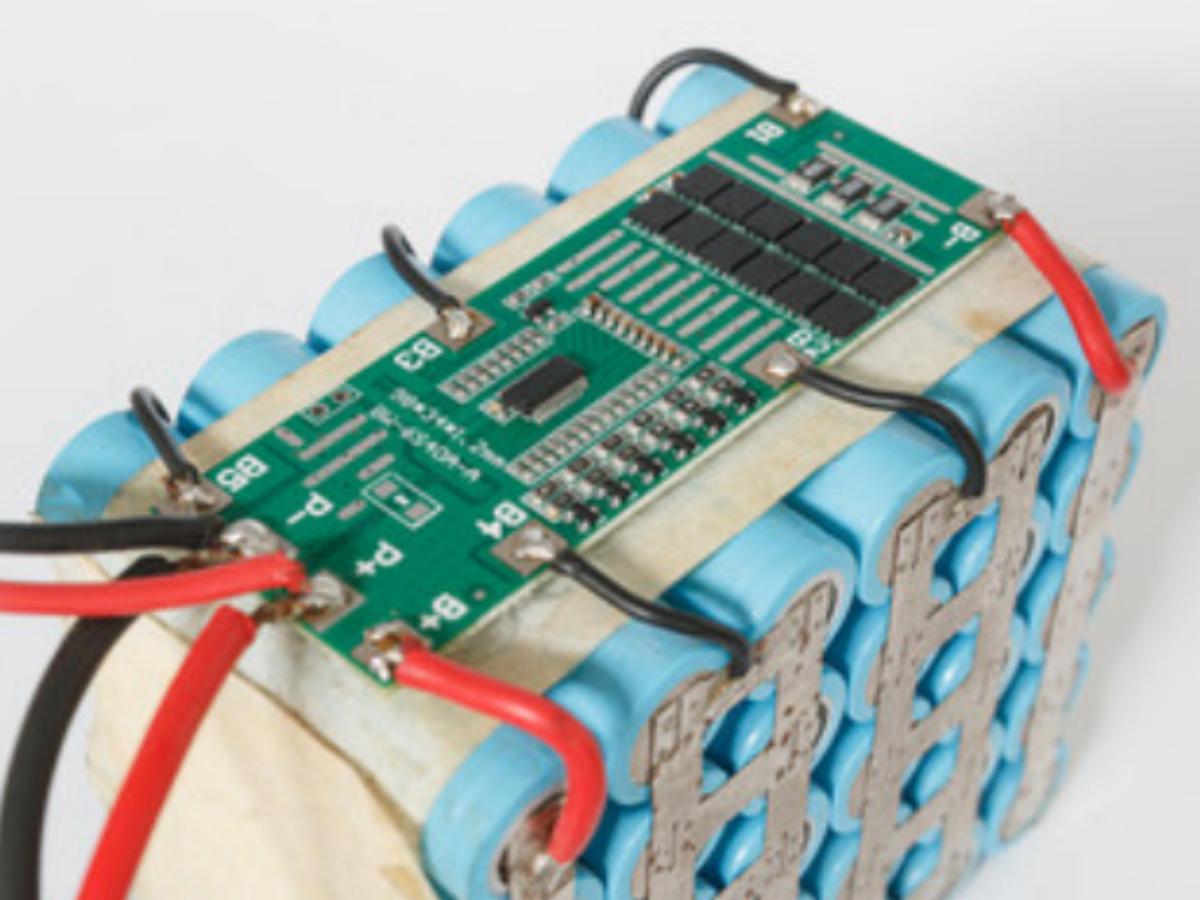
What Do You Need to Consider for Balancing Design?

First is the timing optimization for pin multiplexing. Some AFEs use a design where “voltage sampling pins and balancing pins are multiplexed,” which reduces the IC size but makes it impossible to balance adjacent batteries at the same time. In engineering, you need to schedule the balancing timing through the MCU. Simply put, balance the 1st cell first, then the 2nd cell, with each balancing session lasting 10 minutes. Use time-sharing execution to ensure all batteries can be balanced.
 
The balancing activation condition usually takes “a single-cell voltage difference ≥50mV” or “a SOC difference ≥3%” as the activation threshold to avoid frequent triggering of balancing. For example, when a cell’s voltage is 50mV higher than the average, activate the balancing resistor and discharge until the voltage deviation from the average is ≤20mV. This ensures balancing effectiveness while reducing energy loss.
 
There are generally two implementation paths for passive balancing:
 
  • External balancing: Connect a high-power resistor (e.g., 10Ω/1W) in series outside the AFE. The balancing current can reach 300-500mA, making it suitable for large-capacity battery packs (e.g., ≥10Ah for electric bikes or energy storage). During design, pay attention to resistor heat dissipation—for example, place the resistor on the edge of the PCB and reserve a heat dissipation gap of ≥2mm to prevent the local temperature from exceeding 60°C. At the same time, use the MCU to control the balancing timing, prioritizing execution at the end of charging (SOC ≥90%) to reduce energy waste.
  • Internal balancing: The AFE integrates a balancing resistor, so no additional components are needed, and the BOM (Bill of Materials) cost is low. It’s suitable for small-capacity battery packs. However, the balancing current is smaller, so the balancing time needs to be extended. Additionally, you should pay attention to the AFE’s power consumption control to avoid self-heating during balancing affecting stability.
图片3 22

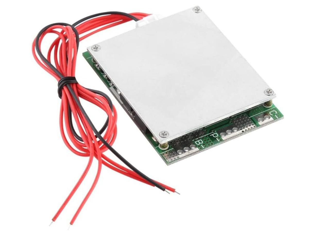
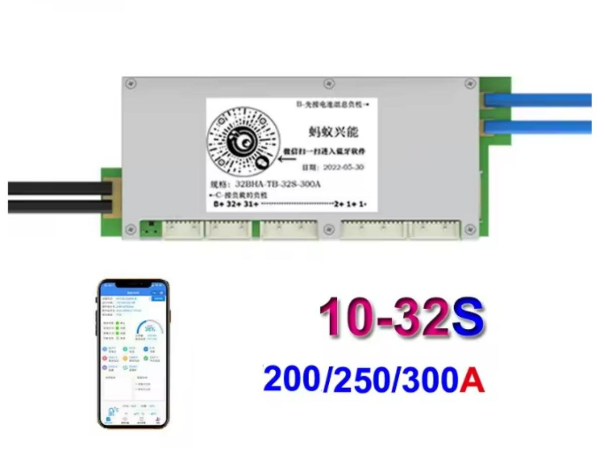
How to Design a BMS Charge-Discharge Circuit?

Which Path Does Current Take During Discharge?

When the load is connected to P+ and P-, the battery supplies power outward. Current flows out from B+ to P+, passes through the load, and flows back to the BMS from P-. Next, it goes through the discharge MOS (Q9) and the sampling resistor R1, and finally returns to B-. At this time, Q9 must be turned on—for an N-channel MOSFET, the condition for turning on is that the gate voltage is higher than the source voltage (you can think of it as the gate needing power to connect the drain and source).

Which Path Does Current Take During Charging?

After connecting the charger, current enters from C+, first passes through the Schottky diode D4 (since it has a small voltage drop, generates less heat when the charging current is large), and then enters the battery B+ (to charge the battery). When the battery is fully charged, current flows out from B-, passes through R1, Q9, and the charging MOS (Q10), and finally flows back to the negative terminal of the charger from C-. At this time, both Q9 and Q10 must be turned on: Q9 allows current to pass through itself after flowing from the B- side through R1, and Q10 sends the current back to the charger.

What Is the Sampling Resistor R1 Used For?

When current flows through it, a voltage is generated (Ohm’s Law: V=I×R). This voltage reflects the current magnitude—the larger the current, the higher the voltage across R1. The capacitor C2 behind it is for filtering; it smooths out current fluctuations, allowing the control circuit to detect the current more accurately (e.g., for sudden inrush currents, the capacitor can buffer the impact).

How Are the MOSFET Controlled?

The gates of Q9 (discharge MOS) and Q10 (charging MOS) have transistors Q1 and Q2 acting as switches behind them. During normal operation, Q1 and Q2 are off, and the gate of the MOSFET is pulled to a high voltage by the internal circuit (meeting the turn-on condition). Once overcurrent or short circuit is detected (e.g., the voltage across R1 exceeds the safe value), the control circuit will apply power to the base of Q1 or Q2, turning them on and pulling down the gate voltage of the MOSFET—the MOSFET then turns off, the circuit is cut off, and the battery and load are protected.

What Are the Protective Components Used For?

  • Diode D4: It conducts unidirectionally! During discharge, the potential of B+ (battery positive) is higher than that of C+ (charger positive), so D4 is reverse-biased and cut off, preventing the battery from discharging into the charger (otherwise, the battery would be drained in reverse).
  • Zener diode D1: It protects Q1. If the voltage output by the control circuit suddenly rises, D1 will break down and clamp the base voltage of Q1 to an appropriate level, preventing Q1 from being burned out.
  • Diodes D5 and D6: They protect the gate of the MOSFET. The oxide layer between the gate and source of a MOSFET is very thin and easily broken down by overvoltage. D5 and D6 act like safety valves—if the gate voltage is too high, they clamp the voltage near the potential of the drain or source to prevent breakdown.
  • Capacitors C1, C3, C4, C5: All are for filtering. C1 and C3 filter out noise on the power line; C4 and C5 stabilize the gate voltage of the MOSFET (preventing the MOSFET from being turned on or off by mistake due to noise).

How to Protect Against Overcurrent?

Suppose the load is short-circuited during discharge—the current suddenly surges, and the voltage across R1 rises sharply. The control circuit detects this abnormal voltage, immediately applies power to the base of Q1, turns on Q1, and pulls down the gate voltage of Q9. Q9 turns off, the discharge circuit is cut off, and the battery won’t be damaged by the large current. The same logic applies to charging: Q2 will cut off Q10 to stop charging.

图片4 11

How Does the BMS Perform Current Sampling?

Low-side sampling connects the sampling resistor R_SHUNT in series between the load and ground. When the load current I_LOAD flows through it, a voltage drop ΔV_SHUNT = I_LOAD × R_SHUNT is generated. The operational amplifier (op-amp) amplifies this voltage differentially and outputs V_O for ADC collection, which is finally used to back-calculate the current value.

Low-Side Sampling

So why low-side sampling? Why place the resistor between the load and ground?
You can think of the circuit as a water flow system: the power supply is a reservoir, the load is a washing machine, and the ground is a sewer. Low-side sampling is like installing a flow meter (R_SHUNT) between the washing machine’s water outlet and the sewer.
 
The lower end of the flow meter is directly connected to the sewer (ground, 0V), and the potential of the upper end changes with the current (V_upper = I×R). The op-amp only needs to process the voltage difference between “upper end → ground,” and the common-mode voltage is close to 0V—something the op-amp can handle easily. (In contrast, for high-side sampling, the flow meter is installed between the reservoir and the washing machine, so both ends have high potentials, and the op-amp has to withstand high voltage, which is both troublesome and costly.) During charging, the current reverses direction (flowing from the sewer → washing machine → reservoir), and the voltage of the flow meter also reverses (positive at the lower end, negative at the upper end). But with the op-amp paired with diodes and a single power supply, it can still measure the current.

Scale: The Sampling Resistor

Think of the current as weight and the sampling resistor as a scale—how to determine the range?
Suppose the battery’s maximum discharge current is 20A. You need to ensure the scale’s voltage drop isn’t too large (which would waste power) or too small (which the ADC can’t detect clearly). For example, if you choose 0.1V as the maximum voltage drop (ΔV_MAX), the resistance value is R = ΔV_MAX / I_MAX = 0.1V / 20A = 5mΩ.
 
To check if it can “withstand the load,” look at the power: P = I²×R = 2W. So the resistor should have a power rating ≥3W (to leave a margin), and you should also choose a manganin resistor (it has small temperature changes, so the “scale” won’t be inaccurate in summer or winter).

Airbag: The Protection Diode

The current may reverse direction (e.g., when the battery is charging), and the sampling voltage will reverse accordingly, which could damage the op-amp. The diode acts as a safety guard.
 
A Schottky diode (e.g., 1N5819) has a small forward voltage drop (≤0.4V) and fast response. It clamps the op-amp’s input voltage near 0V (preventing it from dropping below ground), protecting the op-amp from being damaged by overvoltage.

Filter: The Filter Capacitor

There is high-frequency noise in the circuit (e.g., the hum from switching power supplies), and the capacitor can help filter this out.
 
The feedback terminal C₁₋₁ and R₂₋₁ form an RC filter. Suppose you want to filter out 100kHz noise—set the cutoff frequency to 10kHz (lower than the noise frequency to ensure filtering). Then C = 1/(2πf_c R₂₋₁) ≈ 318pF, so a 330pF capacitor is a good choice. The non-inverting terminal C₁₋₂ works with R₁₋₂; similarly, calculate to get a ≈1.6μF capacitor.

Tips

Note that a +5V power supply is used here, so you need to choose a single-supply op-amp (a dual-supply 5V one won’t work). On the PCB, the high-current power circuit (near the sampling resistor) and the op-amp’s signal circuit should be routed separately to prevent interference from being introduced. The reverse voltage rating of the diode should be higher than the op-amp’s power supply to prevent it from being broken down by surge voltages.

图片5 4

Leave a Reply

Your email address will not be published. Required fields are marked *