Blog
AD7705 AD7606 Data Acquisition Module
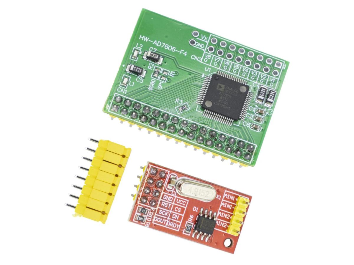
Electronic enthusiasts, rejoice! The AD7705 and AD7606 dual ADC analog-to-digital acquisition module, with 16-bit precision and programmable gain, is here! An industrial-grade masterpiece!
Still struggling with high-precision data acquisition? The AD7705 and AD7606 dual ADC analog-to-digital conversion module is here! It supports 16-bit accuracy, dual-channel input, and programmable gain control, and is suitable for various fields such as industrial control, sensor measurement, and audio processing. This article will take you deep into the performance, advantages, and practical application scenarios of these two amazing analog-to-digital acquisition devices, helping you easily solve the problem of high-precision signal acquisition. Essential knowledge for electronic engineers!
If you are an electronic engineer, embedded development enthusiast, or a person involved in industrial control and sensor measurement, you definitely can’t miss these two modules! They not only support 16-bit high-precision conversion, but also have programmable input gain adjustment, which is simply the “Swiss Army knife of signal acquisition”!
AD7705 Data Acquisition Module
What is AD7705 data acquisition module?
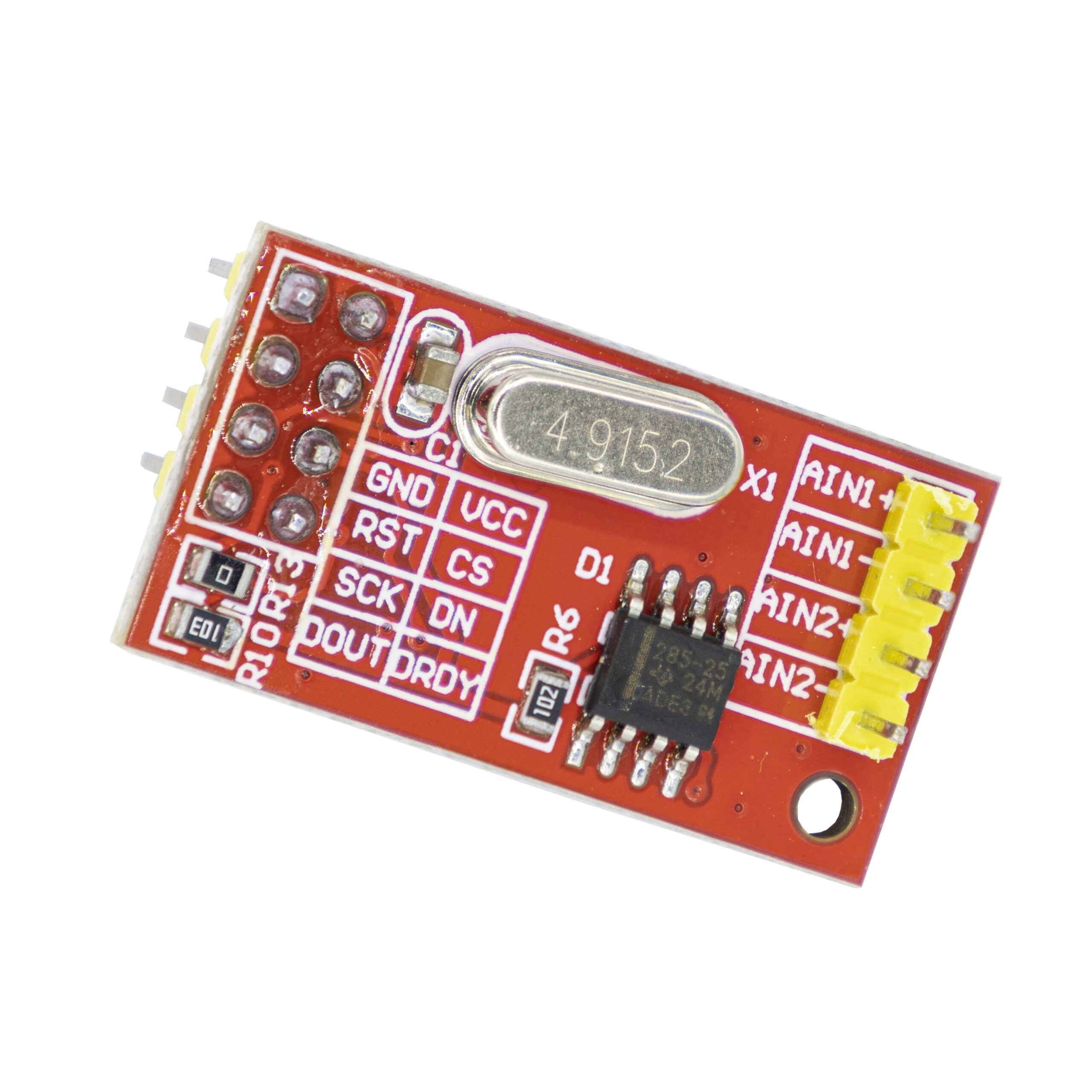
- The AD7705/7706 is a 2/3 channel analog front-end designed for low-frequency measurements. This device can accept low level input signals directly from sensors and generate serial digital outputs. The 16-bit lossless code performance is achieved using the Σ-∆ conversion technology. The selected input signal is sent to a programmable dedicated front-end based on an analog modulator. The on-chip digital filter processes the output signal of the modulator. The cutoff point and output update rate of the digital filter can be adjusted through the on-chip control register to program the first notch of the digital filter.
- The AD7705/7706 requires a single power supply of 2.7~3.3V or 4.75~5.25V. The AD7705 is a dual-channel fully differential analog input, while the AD7706 is a 3-channel pseudo-differential analog input, both with a differential reference input. When the power supply voltage is 5V and the reference voltage is 2.5V, these two devices can process input signals ranging from 0 ~ +20mV to 0 ~ +2.5V. They can also handle bipolar input signals ranging from ±20mV to ±2.5V. For the AD7705, the AIN(-) input terminal is used as the reference point, while for the AD7706, the COMMON input terminal is used. When the power supply voltage is 3V and the reference voltage is 1.225V, these two devices can process single-polarity input signals ranging from 0 ~ +10mV to 0 ~ +1.225V. The bipolar input signal range for the AD7705 is ±10mV to ±1.225V, while for the AD7706 it is ±10mV to ±1.225V. Therefore, the AD7705/7706 can achieve the conditioning and conversion of all signals for the 2/3 channel system.
- The CMOS structure ensures that the device has extremely low power consumption, with the power consumption during the sleep mode reduced to 20μW (typical value). The AD7705/7706 uses 16-pin plastic dual in-line (DIP) and 16-pin wide body (0.3 inch) SOIC packages, as well as 16-pin TSSOP packages.
Working Principle
- AD7705 data acquisition module circuit diagram

- Functional block diagram

The AD7705 mainly operates in differential mode, which involves splitting the input signal into positive and negative parts, then amplifying, sampling, and comparing them to obtain a digital output. Common differential input circuits include the voltage selection type (selecting a fixed resistor) and the dual capacitor coupling type, etc.
- AD7705 chip peripheral circuit diagram

- In-processor register operations
The AD7705 chip includes 8 registers, which can be accessed through the device’s serial port. The first one is the communication register, which manages channel selection, determines whether the next operation is a read operation or a write operation, and decides which register to read or write next. All communication with the device must start by writing to the communication register. After power-on or reset, the device waits for a write operation on the communication register. The data written to the communication register determines whether the next operation is a read or a write, and also decides which register the read or write operation will occur on. Therefore, before writing any other register, one must first write to the communication register, and then write to the selected register.
- Communication Register (RS2=0, RS1=0, RS0=0)
The communication register is an 8-bit register that can both read data and write data into it. All communication with the device must start by writing to this register. The data written onto it determines which register the next read or write operation occurs in. Once the next read or write operation on the selected register is completed, the interface returns the status of a write operation received by the communication register.
① /DRDY:For write operations, a “0” must be written to this bit so that the write operation on the communication register can be accurately completed. If a “1” is written to this bit, the subsequent bits cannot be written into this register. It will remain at this bit until a “0” is written to this bit. Once a “0” is written to the 0/DRDY bit, the following 7 bits will be loaded into the communication register. For a read operation, this bit provides the DRDY flag of the device. The state of this bit is the same as the state of the DRDY output pin.
② RS2 – RS0: Register Selection Bits. These three bits select which of the 8 on-chip registers will undergo the next read/write operation. Once the selected register has completed the read/write operation, the device returns to the state of waiting for the next write operation from the communication register. It will not remain in the state of continuing to access the original register.

③ R/W: Read/Write Selection. This bit determines whether the next operation is to read or write the selected register. “0” indicates write operation, and “1” indicates read operation.
④ STBY: Standby Mode. When this bit is set to “1”, the device is in a waiting or power-off mode. In this mode, the power current consumed by the device is only 10μA. During the waiting mode, the device will retain its calibration coefficients and control word information. When “0” is written, the device is in normal operation mode.
⑤ CH1~CH0: Channel Selection. These 2 bits select a channel for data conversion or access to the calibration coefficients, as shown in the table. The 3 pairs of calibration registers inside the device are used to store the calibration coefficients. As indicated in the figure, which channel combinations have independent calibration coefficients. When CH1 is logic 1 and CH0 is logic 0, as shown in the table, for AD7705/7706, the AIN1(-) input pin is internally short-circuited by itself. This can be used as a test method for evaluating noise performance (without an external noise source). In this mode, the AIN1(-)/COMMON input terminals must be connected to an external voltage within the allowable common-mode voltage range of the device.

- Setup Register (RS2 = 0, RS1 = 0, RS0 = 1)

①MD1、MD0:

②G2-G0:Gain selection bit

③ B/U: Unipolar/Bipolar operation. “0” indicates bipolar operation selection, and “1” indicates unipolar operation.
④ BUF: Buffer control. “0” indicates a short circuit of the internal buffer. After the buffer short circuit, the power current decreases. When this bit is at a high level, the buffer is connected in series with the analog input, allowing high-impedance sources to be processed at the input end.
⑤ FSYNC: Filter synchronization. When this bit is at a high level, the nodes of the digital filter, the filter control logic, and the calibration control logic are in the reset state, and at the same time, the analog modulator is also controlled in the reset state. When it is at a low level, the modulator and the filter start processing data and generate an effective word within 3×(1/Output Update Rate) time (that is, the stabilization time of the filter). FSYNC does not affect the digital interface and does not reset the /DRDY output (if it is a low level).
- Clock register (RS2=0, RS1=1, RS0=0)

① ZERO: Zero must be written at these positions to ensure the correct operation of AD7705/7706.
② CLKDIS: Main clock disable bit. A logic “1” indicates that the main clock is prevented from outputting on the MCLKOUT pin. When disabled, the MCLKOUT output pin is at a low level.
③ CLKDIV: CLKDIV clock divider bit. When CLKDIV is set to logic “1”, the clock frequency at the MCLKIN pin is divided by 2 before being used by AD7705/7706. “1” represents a 2x division, and “0” represents no division.
④ CLK: Clock bit. The CLK bit should be set according to the operating frequency of AD7705/7706. If the converter’s main clock frequency is 2.4576 MHz (CLKDIV = 0) or 4.9152 MHz (CLKDIV = 1), CLK should be set to “0”. If the device’s main clock frequency is 1 MHz (CLKDIV = 0) or 2 MHz (CLKDIV = 1), this bit should be set to “1”. This bit sets the appropriate scale current for the given operating frequency and (along with FS1 and FS0) selects the output update rate of the device.
⑤ FS1, FS2: Filter selection bits, which together with CLK determine the output update rate of the device. As shown in the figure, the first notch and -3dB frequency of the filter are indicated.

- Data Register (RS2=0, RS1=1, RS0=1)
The data register is a 16-bit read-only register that contains the latest conversion results from AD7705/7706. If the communication register sets the device to perform a write operation on this register, a write operation will actually occur to bring the device back to the state ready for a write operation on the communication register, but the 16-bit digital value written to the device will be ignored by AD7705/7706.
- Test Register (RS2=1, RS1=0, RS0=0)
The test register is used for testing the device. It is recommended that users do not change the default values of any bits in the test register (automatically set to all 0 at power-on or reset), otherwise the device will not operate correctly when in test mode.
- Zero-scale Calibration Register (RS2=1, RS1=1, RS0=0), Full-scale Calibration Register (RS2=1, RS1=0, RS0=1) are generally not set.
Feature
- 16-bit lossless code AD converter.
- When the chip is powered by 5V, the recommended REF voltage range is 1V to 3.5V, and the recommended value is 2.5V.
- When the chip is powered by 3V, the recommended REF voltage range is 1V to 1.75V, and the recommended value is 1.225V. The reference voltage chip on the module is REF192-2.048, which is 2.048V. Obviously, neither of these are the recommended values, and this has already exceeded the recommended range for 3V power supply. Therefore, the circuit design is not standardized.
- Dual-channel differential input.
- When the reference voltage is 2.5V, in single-polarity signals, the input range is 0 to 2.5V, and in bipolar input, the input range is -1.25 to +1.25.
- Low-power CMOS chip, with a general power consumption of 20uW.
- Programmable, including programmable gain and noise reduction parameters, etc.
Pin Functions
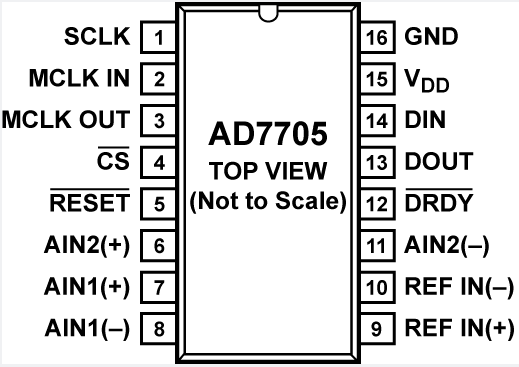
Pin | Function |
SCLK | Serial Clock. An external serial clock is applied to the Schmitt-triggered logic input to access serial data from the AD7705/AD7706. This serial clock can be a continuous clock with all data transmitted in a continuous train of pulses. Alternatively, it can be a noncontinuous clock with the information transmitted to the AD7705/AD7706 in smaller batches of data. |
MCLK IN | Master Clock Signal. This can be provided in the form of a crystal/resonator or external clock. A crystal/resonator can be tied across the Pin MCLK IN and Pin MCLK OUT. Alternatively, the MCLK IN pin can be driven with a CMOS-compatible clock with the MCLK OUT pin left unconnected. The parts can be operated with clock frequencies in the range of 500 kHz to 5 MHz. |
MCLK OUT | When the master clock for these devices is a crystal/resonator, the crystal/resonator is connected between Pin MCLK IN and Pin MCLK OUT. If an external clock is applied to Pin MCLK IN, Pin MCLK OUT provides an inverted clock signal. This clock can be used to provide a clock source for external circuitry and is capable of driving 1 CMOS load. If the user does not require this clock externally, Pin MCLK OUT can be turned off via the CLKDIS bit of the clock register. This ensures that the part does not unnecessarily burn power driving capacitive loads on Pin MCLK OUT. |
| /CS | Chip Select. Active low logic input used to select the AD7705/AD7706. With this input hardwired low, the AD7705/AD7706 can operate in its 3-wire interface mode with Pin SCLK, Pin DIN, and Pin DOUT used to interface to the device. The CS pin can be used to select the device communicating with the AD7705/AD7706. |
| /RESET | Logic Input. Active low input that resets the control logic, interface logic, calibration coefficients, digital filter, and analog modulator of the parts to power-on status. |
AIN2(+) | Positive Input of the Differential Analog Input Pair AIN2(+)/AIN2(−) for AD7705. Channel 1 for AD7706. |
AIN2(-) | Negative Input of the Differential Analog Input Pair AIN2(+)/AIN2(−) for AD7705. Channel 3 for AD7706. |
AIN1(+) | Positive Input of the Differential Analog Input Pair AIN1(+)/AIN1(−) for AD7705. Channel 2 for AD7706. |
AIN1(-) | Negative Input of the Differential Analog Input Pair AIN1(+)/AIN1(−) for AD7705. COMMON input for AD7706 with Channel 1, Channel 2, and Channel 3 referenced to this input. |
REFIN(+) | Reference Input. Positive input of the differential reference input to the AD7705/AD7706. The referenceinput is differential with the provision that REF IN(+) must be greater than REF IN(−).REF IN(+) can lie anywhere between VDD and GND. |
REFIN(-) | Reference Input. Negative input of the differential reference input to the AD7705/AD7706. The REF IN(−) can lie anywhere between VDD and GND, provided that REF IN(+) is greater than REF IN(−). |
| /DRDY | Logic Output. A logic low on this output indicates that a new output word is available from the AD7705/AD7706 data register. The DRDY pin returns high upon completion of a read operation of a full output word. If no data read has taken place between output updates, the DRDY line returns high for 500 × tCLK IN cycles prior to the next output update. While DRDY is high, a read operation should neither be attempted nor in progress to avoid reading from the data register as it is being updated. The DRDY line returns low after the update has taken place. DRDY is also used to indicate when the AD7705/AD7706 has completed its on-chip calibration sequence. |
DOUT | Serial Data Output. Serial data is read from the output shift register on the part. The output shift register can contain information from the setup register, communication register, clock register, or data register, depending on the register selection bits of the communication register. |
DIN | Serial Data Input. Serial data is written to the input shift register on the part. Data from the input shift register is transferred to the setup register, clock register, or communication register, depending on the register selection bits of the communication register. |
VDD | Supply Voltage. 2.7 V to 5.25 V operation. |
GND | The ground potential reference point of the internal circuit. |
Parameters
Model | AD7705 |
Working voltage | 2.7 V to 3.3 V or 4.75 V to 5.25 V |
Power consumption | Maximum 1 mW (3 V) |
Standby current | Maximum 8 µA |
Encapsulated type | 16-pin DIP, 16-pin SOIC and TSSOP packages |
AD7606 Data Acquisition Module
What is AD7606 data acquisition module?

The AD7606 is an 8-channel 16-bit synchronous sampling ADC chip of ADI. The maximum sampling rate can reach 200KSPS. The maximum selectable analog input voltage range is ±5V or ±10V. It is powered by a 5V single power supply. There are two communication interfaces available: parallel port and SPI serial port.

① Parallel port jumper wires: R1 is left unconnected (not soldered), R2 is connected with a 10K resistor.
② SPI interface jumper wires: R1 is connected with a 10K resistor, R2 is left unconnected (not soldered).
This is a particularly user-friendly chip. It enables simultaneous sampling for 8 channels, with each sampling rate being 200KSPS, equivalent to 8 independent single-channel ADCs. Additionally, it only requires a 5V single power supply and can also collect negative voltages, simplifying PCB design.
As shown in the figure below, on the left are the 8 ADC channels. The input clamp protection circuit is ±16.5V, followed by a 1MΩ resistor, meaning the ADC analog input impedance is 1MΩ. Then it passes through an anti-aliasing filter with a cutoff frequency of 22KHz.
The maximum sampling rate of the ADC is 200KSPS. If the collected signal is to remain undistorted in the time domain, it can only be a signal with a frequency of 20KHz or lower (for time-domain sampling to be distortion-free, the sampling rate must be at least ten times that of the sampled signal), and this has no effect.
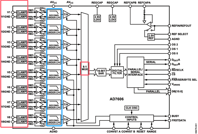
After the 8-channel ADC conversion, one of the ADC’s data is selected by the data selector and transmitted to the communication interface. The following explains this chip based on the schematic diagram.
Working Principle
- ADC working principle:
Sampling: Sampling the analog value -> Holding: Keeping the switch on for a period of time to charge the capacitor to the collected voltage value -> Quantization and encoding: Converting the voltage value into a digital quantity.
- Pin description of AD7606 module
The schematic diagram of the AD7606 module is as follows. This chip does not have configurable registers inside, so it is best to analyze based on the pins. According to the different functions of the pins, it can be roughly divided into power supply, mode configuration, communication interface, and acquisition interface.

AD7606 Schematic Diagram
The AD7606 has many pins. We will select some of the important pins to explain:
Pin | Description |
AVcc | Simulated voltage source, ranging from 4.75V to 5.25V |
AGNG | Grounding |
OS[2:0] | Over-sampling mode pin. Logical input. These inputs are used to select the over-sampling rate. OS2 is the MSB control bit, while OS0 is the LSB control bit. |
PAR(Low level is active)/SER/BYTE SEL | Parallel/Serial/Byte interface selection input. If this pin is connected to a logic low level, then the parallel interface is selected. If this pin is connected to a logic high level, then the serial interface is selected. |
RANG | Select the input range for analog input. If this pin is connected to a logic high level, the analog input range for all channels is +10V. If this pin is connected to a logic low level, the analog input range for all channels is +5V. |
CONVST A / CONVST B | Activate the conversion signal. CONVST A activates channels 1, 2, 3, and 4; CONVST B activates channels 5, 6, 7, and 8. |
RESET | Reset input. When set to a logic high level, the rising edge of RESET resets; the typical width of the high pulse of RESET is 50ns. If a RESET pulse is applied during the conversion, the conversion will be interrupted. If a RESET pulse is applied during the read operation, the content of the output register will be reset to 0. |
RD(Low level is active)/SCIK | When choosing the parallel interface, it is the parallel data read control input (RD_); when choosing the serial interface, it is the serial clock input (SCLK). In parallel mode, if both CS_ and RD_ are at a logical low level, the output bus will be enabled. In serial mode, this pin is used as the serial clock input for data transmission. The falling edge of CS causes the data output lines DoutA and DoutB to exit the tri-state mode, and sequentially outputs the most significant bit (MSB) of the conversion result. The rising edge of SCLK sequentially transmits all subsequent data bits to the serial data output DoutA and DoutB. Reset input. When set to a logic high level, the rising edge of RESET resets; the typical width of the RESET high pulse is 50ns. If a RESET pulse is applied during the conversion, the conversion will be interrupted. If a RESET pulse is applied during the read operation, the content of the output register will be reset to 0. |
CS | Chip Select. This low level signal is effective. In parallel mode, if both CS and RD are at logic low levels, it enables the output of the bus DB[15:0]. In serial mode, CS enables the transmission of serial data frames and outputs the most significant bit (MSB) of the serial output data one by one. |
BUSY | Output busy signal. After both CONVST A and CONVST B reach the rising edge, this pin becomes a logic high level, indicating that the conversion process has begun. The BUSY output remains at a high level until the conversion process of all channels is completed. The falling edge of BUSY indicates that the conversion data is being latched into the output data register, and it becomes available for reading after a time t₄. The data reading operation performed when BUSY is at a high level should be completed before the falling edge of BUSY. When the BUSY signal is at a high level, the rising edge of CONVST A or CONVST B has no effect. |
FRSTDATA | The FRSTDATA output signal indicates when to read back the first channel V1 on the parallel, byte, or serial interface. In parallel mode, the falling edge of the RD signal corresponding to the V1 result will subsequently set the FRSTDATA pin to a high level, indicating that the output data bus can provide the result of V1. After the next falling edge of RD, the FRSTDATA output returns to a logic low level. In serial mode, FRSTDATA becomes a high level at the CS falling edge because at this time the MSB of V1 will be output on DoutA. After the 16th falling edge of SCLK after the CS falling edge, it returns to a low level. |
DB0 – DB15 | Read data bus |
OS[2:0] oversampling mode selection
OS2 ,OS1,OS0 | Description | Maximum rate |
000 | No oversampling | 200Ksps |
001 | Twice the oversampling | 100Ksps |
010 | 4 times oversampling | 50Ksps |
011 | 8 times oversampling | 25Ksps |
100 | 16 times oversampling | 12.5Ksps |
101 | 32 times oversampling | 6.25Ksps |
110 | 64 times oversampling | 3.125Ksps |
111 | Ineffective |
- Analysis and Implementation of Parallel Mode Timing for AD7606
Parallel Mode Timing Diagram


Parallel mode timing requirements
Time Name | Time Duration | Description |
tRESET | 50ns | Minimum width of high level reset |
t2 | 25ns | The shortest width of the CONVST low level pulse |
t7 | 25ns | The shortest width between the low level of RESET and the high level of CONVST |
t5 | 0.5ns | The shortest delay time between the rising edges of CONVSTA and CONVSTB |
t1 | 40ns | The maximum delay time between the rising edge of CONVST and the rising edge of BUSY |
tCYCLE | 5ns | The longest delay time between the rising edge of CONVST and the next rising edge of CONVST |
t3 | 25ns | CONVST high level minimum time |
t4 | 0ns | The shortest time from the rising edge of BUSY to the rising edge of CS |
t8 | 0ns | The shortest time between the falling edge of CS and the falling edge of RD |
t10 | 16/21/25/32ns | The width of the low level pulse in the RD signal is determined based on the Vdrive level. |
t11 | 15ns | Minimum width of the low level pulse in the RD signal |
t9 | 0ns | The minimum time from the rising edge of RD to the rising edge of CS |
tCONV | 3.45ns | The conversion time is at least 3.45 microseconds and at most 4.15 microseconds. |
Feature
- Use the AD7606 high precision 16-bit ADC chip
- 8 analog inputs. Impedance 1M Ohm. (No need for negative power supply, no need for front-end analog amplifier circuit, can directly connect to sensor output)
- Input range ±5V, ±10V. Can be controlled by IO to set the range.
- Resolution 16 bits.
- Maximum sampling frequency 200Ksps. Supports 8-level oversampling settings (can effectively reduce jitter)
- Built-in benchmark
- 5V power supply
- SPI interface or 16-bit bus interface. Interface IO level can be 5V or 3.3V
AD7705 VS AD7606
Feature | AD7705 module | AD7606 module |
ADC Type | Σ-Δ (Sigma-Delta) | SAR (Successive Approximation) |
Resolution | 16-bit | 16-bit |
Channels | 2 (Fully Differential) | 4/6/8 (True Differential, model-dependent) |
Max Sampling Rate | 500 Hz | 200 kSPS |
Input Range | ±2.5V (Programmable via PGA) | ±10V / ±5V (Fixed, no PGA) |
Power Supply | 2.7V–5.25V (Single Supply) | ±12V (Analog) + 5V (Digital) or Single 5V |
Power Consumption | 1 mW | 142 mW |
Operating Temp. | -40°C to +85°C | -40°C to +85°C (Extended to +125°C at ≤160 kSPS) |
Interface | SPI (3-Wire) | SPI/Parallel (Flexible) |
Key Applications | Low-Speed Sensors (RTD, Strain Gauge) | High-Speed DAQ (Power Monitoring, Industrial Control) |
Special Features | On-Chip PGA (Gain: 1–128), Self-Calibration | Integrated Ref. Buffer, Oversampling Filters |
Module Function
- Data acquisition: The data acquisition module is responsible for collecting data from various data sources, which can be either real-time or offline.
- Data transmission: The data acquisition module sends the collected data through the transmission interface to the backend system.
- Data processing: The data acquisition module conducts preliminary processing on the received data, such as cleaning, noise reduction, and formatting, to prepare for subsequent analysis.
- Data storage: The data acquisition module stores the processed data in local or cloud-based databases for subsequent querying and usage.
- Data analysis: The data acquisition module supports various data analysis methods, such as statistical analysis, machine learning, and deep learning, to help users extract valuable information from massive data.
- Data visualization: The data acquisition module provides a variety of data visualization tools, such as charts, maps, and dashboards, to help users present data and trends in an intuitive manner.
Application Scenarios
- Internet of Things: A large amount of data generated by IoT devices needs to be collected and processed through data collection modules in order to achieve remote monitoring and management of the devices.
- Industrial Automation: Sensors and actuators in industrial production generate a large amount of real-time data. Data collection modules can collect this data in real time and perform analysis to improve production efficiency and product quality.
- Smart Cities: Various sensors and cameras in cities generate a large amount of data. Data collection modules can collect and process this data to support urban planning and management.
- Financial Risk Control: Financial institutions need to monitor and analyze real-time data of customers’ transaction behaviors and credit status to provide better services.
- Medical Health: Medical institutions need to collect and analyze data such as patients’ physiological parameters and medical records to provide better medical services.
- Transportation Logistics: Logistics companies need to monitor and analyze information such as vehicle locations, speeds, and goods, and data collection modules can help logistics companies improve operational efficiency and service quality.
- Energy Management: Energy companies need to collect and analyze data such as the operation status of the power grid and equipment performance to optimize energy allocation and reduce operating costs.
Relative Information
Module Purchase Link
FAQ
What is ADC in data acquisition system?
Analog-to-digital converters (ADCs) and digital-to- analog converters (DACs) play an important role in the design of data acquisition systems. ADCs are used to convert analog signals like the output from a temperature transducer, a radio receiver or a video camera into digital signals for processing.
Why is ADC used?
An ADC converts a continuous-time and continuous-amplitude analog signal to a discrete-time and discrete-amplitude digital signal. The conversion involves quantization of the input, so it necessarily introduces a small amount of quantization error.
What does a data acquisition module do?
A DAQ (Data Acquisition) system is a set of components and devices used to measure and collect data from various sensors or transducers. It involves the conversion of physical or electrical signals into digital data for further analysis and processing.

